Monday, March 21, 2011

Panasonic Gate-First HKMG also First Out of the Gate

As I suggested a few months ago, we put some credence in Panasonic’s press release last September that they would be shipping their first 32-nm HKMG parts last October. Samsung had announced their Saratoga chip, and both Altera and Xilinx have displayed silicon from TSMC, but until last Friday (18 March), none have said that they were shipping product. As of Friday Xilinx announced that they were shipping their Kintex-7 product, the first of their 7-series of FPGAs.

Earlier this month our faith in Panasonic was rewarded, and we found the chip! It took a few false starts buying Panasonic products that we tore down and threw away, but now we have a verified 32-nm, gate-first, high-k metal-gate (HKMG) product. The supply chain was a bit longer than we had hoped, but as promised the chip was shipped with a week 41 date code, in October.

So, for the curious, this is what a transistor looks like:

Panasonic's 32-nm HKMG NMOS Transistor

We can see the TiN metal gate at the base of the polysilicon, and the thin line of high-k at the base of the TiN. Also noticeable are a dual-spacer technology (sometimes referred to as differential offset spacers), and a thin line of nitride over the source/drain extension regions (possibly indicating a nitrided oxide under the high-k). The salicide is the usual platinum-doped nickel silicide. Less visible are mechanisms of applying strain, other than the nitride layer over the gate; embedded SiGe and dual-stress liners are not used.

All of which is typical for Panasonic – their 45-nm product did not appear to use any enhanced strain techniques, and the only concession to PMOS enhancement was wafer rotation to give a 1-0-0 channel direction. The emphasis is different from Intel; rather than raw performance, the targets are increased integration, die size reduction/reduced cost, and now we have high-k, reduced leakage/lower power. The September press release does say that transistor performance is improved by 40%, but it also claims 40% power reduction and a 30% smaller footprint.

Here’s a 45-nm transistor for comparison:
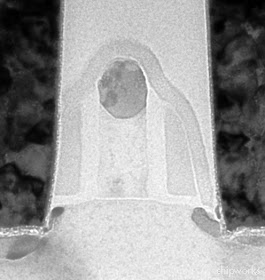
Panasonic's 45-nm Generation Transistor

And, for good measure, Intel's 32-nm device:

Intel 32-nm NMOS Transistor

The part itself uses a nine-metal (eight Cu, one Al) stack with a hybrid low-k/extra-low-k stack. Die size is ~45 mm2 in a conventional FC-BGA package. Minimum metal pitch is specified as 120 nm [1], and we have found 125 nm in our early investigations.

Panasonic 32 nm General Structure

Analysis is ongoing – stay tuned for more details, and of course we’ll be doing reports!

[1]S. Matsumoto et al., Highly Manufacturable ELK Integration Technology with Metal Hard Mask Process for High Performance 32nm-node Interconnect and Beyond”, IITC 2010

Sunday, March 13, 2011

Apple's A5 Processor is by Samsung, not TSMC

Forty-eight hours ago we obtained an iPad 2 and brought it back to the lab, and took it apart to have a look at Apple's A5 processor chip. We've come to the conclusion that the main innovation in the new iPad is the A5 chip. Flash memory is flash memory (multi-sourced from Samsung and Toshiba in the iPads we've seen), the DRAM in the A5 package is 512 MB instead of 256 MB, and the touchscreen control uses the same trio of chips as the iPad 1 – not even a single chip solution as we’ve seen in the later iPhones. And the 3G version uses the same chipset as the Verizon iPhone launched a few weeks ago. This is the mother-board from a 32-GB WiFi-only iPad 2:

Motherboard from 32-GB iPad 2


The A5 can be seen in the centre of the board. If we look at the package we can identify the Apple's APL0498 marking for the A5 (the A4 is APL0398), and also 4 Gb of Elpida mobile DRAM. Date codes are 1107 for the A5 and 1103 for the memory - only a few weeks in the supply chain here!


Apple A5 from iPad 2


The x-ray images show us that we have the usual package-on-package (PoP) structure, with two memory chips in the top part of the PoP, and the APL0498 processor on the lower half.


X-Ray Image of A5 Package-on-Package

The two rows of dense black dots on the outside of the image are the solder balls from the memory chips in the top half of the package (connecting with the bottom half), and the less dense dots are the solder balls on the bottom half of the package connecting the A5 chip to the iPad board below. If you squint really hard you can see smaller dots about five rows in from the edge which are the flip-chip solder balls on the A5 die – and they take up quite a large proportion of the area, showing that this is a good-sized die.
The die photo and die mark are shown here:
Die Photo of Apple's A5 Chip from the iPad 2

APL0498E01 Die Mark of Apple A5 Chip


The x-ray is right – the A5 die is more than twice as large as the A4, at 10.1 x 12.1 mm (122.2 mm2), vs 7.3 x 7.3 mm (53.3 mm2) – here’s the A4 chip for comparison:
Apple A4 Die Photo


Given that the A5 is a dual-ARM core, and has more graphics capability than the A4, more than doubling the size is to be expected, but it’s also a clue that this is still made in 45-nm technology.
So after the web speculation that TSMC might be fabbing the A5 rather than Samsung, we had to take a look, and the quickest way is to do a cross-section and compare it with the A4 from last year’s iPad.
So here’s the A5:
SEM Cross-Section of Apple A5
It’s a nine-metal layer part, with eight levels of copper and one aluminum. Zooming into the transistor level:
SEM Cross-Section of Transistors and M1 in A5 Processor
And now the A4:

SEM Cross-Section of Transistors and M1 - M4 in A4 Processor

At this scale even electron microscopes start to run out of steam, so not the clearest of images in either case, but good enough to see the similar shape of the transistor gates and the dielectric layers. So at least this sample of the A5 is fabbed by Samsung, just as all Apple’s processor chips have been for the last while.

Many thanks to the guys in the lab who've worked through the weekend to get this information - Chipworks is not really in the media business, but there's always a buzz when a hot new consumer part comes out.

And on a different note, commiserations and condolences to our Japanese colleagues, they have much more important things of concern than the details of the iPad 2.