At a morning session at the Intel Developer Forum Tuesday, Mark Bohr tooted the Intel trumpet and put a slide up to emphasise their lead over the other leading semiconductor companies:
 |
| Intel Process Evolution Since 90-nm |
One can quibble a bit about the odd month here or there for the dates, but essentially things have been as they say -- they were the first with embedded SiGe for PMOS strain, they were a node ahead of everyone else at HKMG, and if the trigate launch comes to pass as planned at the end of this year, they will be years ahead with their version of the FinFET.
The main focus of the talk was Intel's upcoming 22-nm trigate transistor technology to be used for the Ivy Bridge processors due out in the New Year. Essentially it was a re-run of the May announcement, with a little more about the SoC version and a look forward to 14-nm in (presumably) 2013.
 |
| Intel Schematic of Trigate Transistor in Inversion |
 |
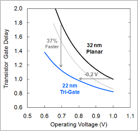
| Transistor Delay vs Voltage (pale grey line is planar 22-nm) Source: Intel |
Mark said that they made the choice for trigate back in 2008, when it became clear that the performance benefit from the fully depleted triple-gate structure (compared to 22-nm planar) was significant enough to justify the additional effort and cost of another step-function change in process architecture.
Compared with the 32-nm equivalent, the trigate gives a 37% performance increase at a lower voltage or a 50% power reduction at constant performance. Somehow Intel does this with no extra mask levels and only 2-3% additional cost (although extra litho steps are used, because of the need for double patterning).
Of course, I was keen to hear when we'll be able to get hold of some of these chips, after all they're going to be fascinating to take apart!. According to Mark, they are "just about ready to start production" in Q4, with public availability in the first half of next year. They are definitely sampling, since Ivy Bridge Ultrabooks are on show here. The strict two-year clock appears to have slipped slightly, since previous launches have been in November; but we quibble, since Intel has a clock -- their competitors make an announcement, and then we wait!
Which brings us to the roadmap; as you can see in the first graphic above, 14 nm is predicted in 4Q13 (which is itself a subtle change, since it was 15-nm a couple of years ago -- Intel seems to be aligning itself with the other companies which have gone the 28 -- 20 -- 14 nm route).
Intel is also continuing the parallel development of SoC processes down to 14 nm:
 |
| New Process Roadmap Source: Intel |
Given the extension to 14 nm, Intel must have already verified that the transistor-related SoC features (low leakage and high-voltage transistors, and the different varieties of SRAM) work with trigates, the rest are all back-end related so should just suffer the normal scaling problems.
Unfortunately it appears that there will not be a paper on the 22-nm process at IEDM this year, so we will have to wait for Ivy Bridge chips to come on to the shelves to get a few more clues -- it should be an interesting spring!