Telling it like it is on the inside of production semiconductors as seen at Chipworks


Tuesday, October 2, 2012

GLOBALFOUNDRIES takes on Intel with 14nm finFET “eXtreme Mobility” process

A week after Intel were claiming that their 14nm process will be ready to go at the end of next year, GLOBALFOUNDRIES (GF) announced that they will have a 14nm finFET process for launch in 2014. Unfortunately they timed it to coincide with the iPhone 5, so we at Chipworks were tied up for a few days tearing it down.

However, I don't want to ignore this development -- it could make the 2014 an interesting year! GF have dubbed the new process 14XM, for "eXtreme Mobility," since from the start it has been targeted on mobile applications -- after all, mobile products are the volume driver in the chip business these days.

And what's the biggest complaint from mobile users? Having to charge them so often, as battery technology has not improved at anything like a rate comparable to chip performance.


So while GloFo got started in high-k metal-gate (HKMG) making 32nm parts for AMD, they have seen the obvious and are generating low-power processes, beginning with the 28-SLP, moving to the 20-LPM, and now the 14XM.

The 20-LPM process claims a 40% reduction in power from the 28nm generation, and the 14XM claims 40%-60% increased battery life over 20-LPM. The 20nm generation is scheduled for next year, and as noted earlier 14XM is due out in 2014, a year later, breaking the two-year cadence that we've all got used to. Apparently 20nm wafers are running the full process in the Malta, NY fab right now.


They're accelerating the process launch by using the 20-LPM middle/back end-of-line metal stack with the finFET front end. In the 20nm process the 1x metal pitch is 64nm and the single-patterned metal is 80nm -- coincidentally, the latter is the same as Intel's tightest pitch in their 22nm product.

20nm metal pitches shown at the 2012 Common Platform Tech Forum (CPFT)

The use of the 3D finFET structure enables a higher performance/unit area, or lower power/unit area at a given performance at the transistor level. The graph below shows some estimates made by their R&D group.
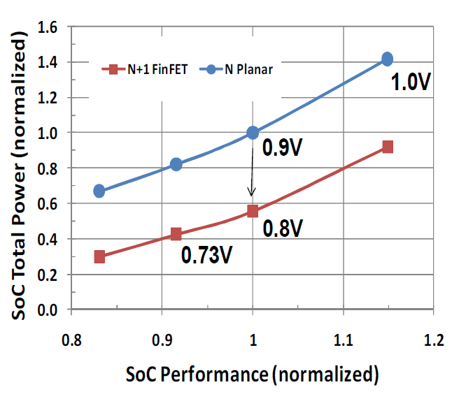
SoC Performance vs. power -- lower power at constant frequency [1]

Functional scaling itself will be limited to some extent by the 20-LPM metal density, but presumably some die shrink can be achieved by using more metal layers, and also the increased current density will allow some compaction since higher-current transistors will be smaller. Keeping single patterning will mitigate the cost, compared with double patterning for denser layers.

The process will also continue from the 20-LPM process in that it will use gate-last (replacement metal gate) technology on a bulk substrate. The R&D group in New York has published a couple of papers [2, 3] referencing a 40nm fin pitch, but 14XM will have a fin pitch of 48nm to leave some slack in the lithographic challenge, and minimize quantization errors. Together with the metal pitches of 64 and 80nm, it implies a 16nm grid as a basis for layout. The use of 64nm Metal 1 presumably also means that the contacted gate (CG) pitch will be 64nm.

The Intel 22nm process has a fin pitch of 60nm, and a CG pitch of 90nm, so it's not unreasonable to assume that their 14nm process will have similar numbers.

We will see whether the fin will be tapered similar to Intel's; these images (below) from CPTF seem to show a vertical fin atop the STI profile, but then, they are only schematics. Using a single (STI) etch to shape the fins (as I think Intel does) should certainly be less complex than trying to get vertical-walled fins on top of the STI trench sidewall.


The economic challenge in going to 14nm is almost as huge as the technical challenge, and keeping the cost/power/performance (CPP) metric in check as process complexity spirals upwards has caused inevitable concern. In particular, the cost benefits of shrinking die size tends to go away as the lithography demands double, triple, and even quadruple patterning.

Jen-Hsun Huang of Nvidia has publicized his concern about increasing wafer costs at last year's IPTC (International Trade Partner Conference) meeting -- the plot below shows the increasing gap in wafer cost between successive nodes:


So if GLOBALFOUNDRIES, or any other foundry, wants to keep the customers coming, they have to mitigate the cost increase going to the next node. Taking a hybrid approach such as the 14XM process should be an attractive option for their existing and future customers.

It's interesting to note that TSMC has changed tack slightly and are now saying that they will be using finFETs at 16nm, not 14nm. They are also claiming that their 20nm metal pitch is leading-edge at 64nm, although that's the same as GF's. It's tempting to wonder if TSMC will also use a hybrid approach and transfer their 20nm back-end to the 16nm node, since the arguments are the same. Chenming Hu thinks so, anyway. TSMC are predicting 16nm risk production in 2014.

We'll see if GF can match Intel's timing -- Mark Bohr sounded very confident at the Intel Developer Forum, when he said their 14nm product would be ready for the tail end of next year. Will we have GF-produced finFETs in early 2014? And will their finFETs be better than Intel's?

My thanks to Subi Kengeri for clearing up some of the technical details.

[1] A. Keshavarzi et al., Architecting Advanced Technologies for 14nm and Beyond with 3D FinFET Transistors for the Future SoC Applications, Proc. IEDM 2012, pp. 67-70.

[2] T. Yamashita et al., Sub-25nm FinFET with Advanced Fin Formation and Short Channel Effect Engineering, Proc. VLSI 2011, pp. 14-15.


[3] C.-H. Lin et al., Channel Doping Impact on FinFETs for 22nm and Beyond, Proc. VLSI 2012, pp. 15-16.

Tuesday, July 10, 2012

The Elephant Has Left the Room – 450 mm is a Go!

It's the day before Semicon opens up, and we have had a slew of announcements on 450 mm, the biggest of which was the joint ASML/Intel notice that Intel will be taking a share of ASML as a way of funding 450 mm and EUV R&D. Simultaneously imec released that the Flemish government would invest in their upcoming 450-mm facility, and imec and KLA-Tencor declared that a 450-mm capable SP3 450 unpatterned wafer defect inspection tool had been installed at imec.


ASML announced it as a “co-investment program” in which Intel would invest EUR829 million (about $1B) over the next five years, EUR553M of which would be in 450 mm R and D. Intel focused more on the R and D and described the financial details later.


They cited the classic economics of doubling the wafer size, and the potential die cost reduction:


All of which is logical, but ASML has been notably reticent about making any comments on 450-mm R and D in the past, to the point where some industry watchers (including me) have wondered if we would ever get there; if the biggest litho vendor isn’t on board, there won't be any 450-mm fabs even if all the other equipment companies are ready.

Which brings me to the elephant in the title. Last year at Semicon there was a 450 mm panel, and everyone was pontificating wisely, until Bob Johnson of Gartner commented on "the elephant in the room - ASML has no 450-mm program, so why are we bothering to even talk about it?" (my paraphrasing). Which kind of shut the whole thing down.

However, that particular pachyderm has clearly moved on, and we have an ASML roadmap with both 450 mm and EUV in it:


We won’t have any production tools until 2018, but at least a huge barrier to adoption is lifted; now there are just the simple engineering tasks of getting a substrate the size of a turkey platter exposed with patterns with feature sizes of 14nm or smaller. Has anyone said that this industry is crazy?

By coincidence Mike Splinter of Applied Materials was speaking at the imec Technology Forum, and he commented that 300-mm had just about paid off its development costs as of now, roughly 14 years after the launch of the first systems. He guesstimated the costs for developing 450 mm as $15 - 20B, with an as yet unknown payoff time. (Has anyone said that this industry is crazy?) However,  he also said this time last year that Applied would spend over $100M on 450 mm and that "450 mm is going to happen."

Clearly Intel has recognised that if it wants 450 mm to go forward, then it has to pony up some cash to encourage the litho side, and it is already invested in the consortium being set up at Albany. For anyone interested in the financial side of the deal, check out the press releases linked above, or watch ASML CFO Peter Wennink in a video.

Looks like 450 mm is actually going to happen!

Friday, July 6, 2012

Sony’s PS Vita Uses Chip-on-Chip SiP – 3D, but not 3D

At the tail end of last year Sony released their PlayStation Vita, and it was duly torn down by iFixit and others. In due course we took it apart too, though we didn’t post it on our teardown blog.

Sony CXD5315GG in the PlaySation Vita
Inside we found the usual set of wireless chips, motion sensors, and memory, but the key to the increased performance of the PS Vita is the Sony CXD5315GG processor, a quad-core ARM Cortex-A9 device with an embedded Imagination SGX543MP4+ quad-core GPU.

Above I said that we found memory, but actually the only discrete memory that we found on the motherboard was 4 GB of Toshiba flash; and Sony’s specification states that there is 512 MB (4 Gb) regular RAM, plus 128 MB (1 Gb) VRAM (video RAM). In a phone that would tell me that there is memory in a package-on-package (PoP) configuration, mobile SDRAM in the top part and the processor in the bottom part.

However, when we took the part off the board and did a set of x-rays, the side view proved me wrong – it’s a stack, and the close-up shows that there appear to be five dies in there, a thick die at the base, a thinner one immediately on top and three smaller die on top of that. The second die down could be a spacer, since there don’t seem to bond wires going to it.
Side x-ray images of Sony CXD5315GG
This immediately led us to speculate – if the second die up is the VRAM, is it wide I/O DRAM, and is it using through-silicon vias (TSVs)? Time for a real cross-section to check that out, and almost predictably we were disappointed:

Sony CXD5315GG package cross-sectioned
This type of face-to-face connection showed up back in 2006 in the original Sony PSP, and Toshiba had dubbed it “semi-embedded DRAM”, now they are calling it “Stacked Chip SoC”. The ball pitch is an impressive ~45 µm, almost as tight as TI’s copper pillars, but they are staggered to achieve 40-µm pitch.

So what are the five chips that are in the stack? At the base we have the processor chip; face to face with it is a Samsung 1-Gb wide I/O SDRAM; and the top three dies comprise two Samsung 2-Gb mobile DDR2 SDRAMs, separated by a spacer die, and conventionally wire-bonded. The base die is ~250 µm thick, and the others ~100 – 120 µm.

When we look at the die photos of the processor and the 1-Gb memory, we can see that they are purposely laid out for the stacked-chip configuration, since in the centres of both is an array of matching bond pads.

Die photos of the Sony CXD5315GG (left) and Samsung 1-Gb wide I/O SDRAM with bond pad arrays annotated
Close examination reveals that there are 1080 pads in two blocks of 540 (2 sub-blocks of 45 rows of 6 pads), so likely 2 x 512 bit I/O operation, possibly sub-divided into 4 x 128.

Wide I/O bond pad arrays in Sony CXD5315GG (top) and Samsung SDRAM
Last year at ISSCC Samsung described a similar wide I/O DRAM using TSVs [1], claiming a data bandwidth of 12.8 Gb/s, four times the bandwidth of an equivalent LPDDR2 part. I doubt that the authors expected their design to be in a volume consumer device before the end of the year, but that seems to be what happened!

Chip architecture of Samsung 1Gb Wide-I/O DRAM and SEM image of microbumps (Source: Samsung/ISSCC)
This uses similar I/Os, but not the same as, the JEDEC wide I/O standard issued earlier this year (which calls for 50 rows of 6 pads in each block), and of course it predates it by about a year.

By combining the processor with the different memories in the same package in the Vita, Sony and Toshiba have produced one of the few true system-in-package (SiP) parts that we have seen. And I would call it 3D, even though industry convention is now restricting that term to TSV-based parts – so it’s not 3D, in our current argot.

In a way this device highlights the commercial barriers to introducing TSVs into the SiP world, since not only do the corresponding parts have to be designed to suit the I/Os, but at least for a two-stack the technology is already there; so the performance cost/benefit has to be critical enough to require TSVs for that third and more die. Admittedly the demands on mobile devices are increasing at an astounding pace, but it still seems a while before we’ll see TSVs in commercial devices. Time will tell!

[1] J-S. Kim et al., A 1.2V 12.8GB/s 2Gb Mobile Wide-I/O DRAM with 4×128 I/Os Using TSV-Based Stacking, ISSCC 2011, pp. 496 – 498.

Tuesday, April 24, 2012

Intel’s 22-nm Trigate Transistors Exposed

Last week Intel had their Q1 conference call for financial analysts, and revealed that the 22-nm Ivy Bridge parts would make up 25% of their shipment volume in the second quarter of this year.  That means that a good quantity will already will have shipped, and we managed to track some down in Hong Kong a few weeks ago.  Of course we got in touch ASAP and the parts duly arrived, and they were the real thing.

Fig. 1 Intel Xeon E3-1230V2 Server CPU

We obtained samples of Xeon E3-1230 v2 CPUs, which are four-core, 3.3 GHz, 64-bit parts intended for the server market. Here is a die photo of the transistor level, with annotations from Intel's Ivy Bridge launch yesterday:

Fig.2 Intel Xeon E3-1230V2 Die

A quick cross-section reveals that Intel have stayed with the nine metal layers used in the last two generations:

Fig. 3 Intel Xeon E3-130V2 General Structure
A closer TEM image (Fig. 4) shows the lower metal stack and a pair of multi-fin NMOS and PMOS transistors. This section is parallel to the gate, across the fins, and we can see the contact trenches and metal levels M1 up to M5.

We have to digress here a little to explain what we’re looking at.  A typical TEM sample is 80 – 100 nm thick, to be thin enough to be transparent to the electron beam and at the same time have enough physical rigidity so that it does not bend or fall apart.

Here we are trying to image structures in a die with a gate length of less than 30 nm; so if we make a sample parallel to the gate, and if the sample is aligned perfectly along the centre of the gate, then it will contain the gate plus at least part of the source/drain (S/D) silicon and contacts on either side.

Fig. 4 TEM Image of Lower Metals and NMOS and PMOS (right) Transistors
That is what we see above – I have labeled the gate and contact stripes, and we have PMOS on the right and NMOS on the left.  The tungsten-filled contacts obscure parts of the gate, but we can clearly see that the PMOS S/D fins have epitaxial growth on them, and the fins have an unexpected slope – a little different from Intel’s tri-gate schematic shown last year –see Fig.5.
Fig. 5 Intel Schematic of Tri-Gate Transistor
If we zoom in a bit further into the PMOS gate (Fig. 6), we can see how the gate wraps over the fin, and the rounded top of the fin.  The thin dark line adjacent to the fin is the high-k layer and just above that is a mottled TiN layer that is likely the PMOS work-function material, as in the 32-nm and 45-nm parts.

Fig. 6 TEM Image of PMOS Gate and Fin Structure
Fig. 7 shows a section of an NMOS transistor.  There is a ‘ghost’ of the contact behind the gate, but the gate structure itself looks similar to the PMOS, with the exception of the work-function material just above the high-k layer (as expected).

Fig. 7 TEM Image of NMOS Gate and Fin Structure
Fig. 8 gives me an opportunity to show off our new TEM – we have recently purchased an FEI Osiris machine, which upgrades our capability considerably. Here we have a lattice image of a fin in an NMOS transistor; the diamond-like layout of the pattern of dots is actually created by the columns of atoms in the silicon crystal lattice. This tells us that the sample is oriented in the <110> direction, which given that silicon has a face-centred cubic structure in which equivalent planes are at right angles, means that the channel direction is also <110>.

Fig. 8 TEM Lattice Image of NMOS Fin Structure
To fully understand what we’re looking at, of course, we need to see what’s happening in the orthogonal direction, along the fin and cross-sectioning the gate – as in Fig. 9. This shows an array of PMOS transistors over a single fin, four functional gates and two dummy gates at the ends of the fin. Again the TEM sample is thick compared with the feature size, so we are seeing the gate on the side(s) of the fin, not just the top. The fin ends have the same taper as in Figs 6 and 7.

Fig. 9 TEM Image of PMOS Transistors
As announced by Intel, there is embedded SiGe in the source/drains, although not etched to the <111> planes as in the 32- and 45-nm product. It also looks as though the tops of the gates have been etched back and back-filled with dielectric, and the contacts are self-aligned as in memory chips.

Zooming in on the PMOS transistor in Fig.10, the image is a bit fuzzy, but the SiGe is clearly in a rounded cavity with no facets on the top, though there are facets on the sides of the fin (see fig. 4).

Fig. 10 TEM Image of PMOS Transistor
Looking at the NMOS equivalent (Figs. 11 and 12), we see a similar structure – there seems to be an epitaxial interface, and the silicide(?) seems to protrude slightly above the fin.

Fig. 11 TEM Image of NMOS Transistors
Fig. 12 TEM Image of NMOS Transistors
 It is hard to say much about the gates here, either NMOS or PMOS, because of the sample thickness problem; we are viewing a slice that includes the gate on both sides of the fin and the fin itself. Fortunately we have images of gate metal over STI and they are less confusing. 

Figure 13 is a composite image of NMOS and PMOS gates so that the differences are highlighted. The dark line surrounding the gate structures is the Hf-based high-k, and within that are the two work-function materials, likely TiN for PMOS and TiAlN for NMOS. (The columnar structure of the PMOS TiN is visible in the right half of the image.)

Fig. 13 Composite TEM Image of NMOS/PMOS Gates
The fill has been changed from TiAl in the earlier parts to tungsten. It is more prominent in the NMOS gates than the PMOS, because the PMOS structure includes both work-function metals, whereas the TiN has been etched out of the NMOS gates. At the 45-nm node Intel used tensile tungsten in the contacts to apply channel stress – have they transposed this to the gates in the 22-nm process?

Just to finish up, so that this is still a blog, not a paper (I don’t want to go on too long) – fig. 14 shows a sample delayered to expose the transistors, and imaged on a tilt angle.  Both the gates and the fins show up nicely, and we can actually see tiny spikes of SiGe in the PMOS source/drains. The small pillars in between the fins in the NMOS areas are residual bits of contact metal.  I think it’s a cool image!

Fig. 14 Tilt SEM Image of NMOS/PMOS Transistors
We are just getting into the full scope of the analysis, so likely more to come in the next few weeks!
I'm still tweeting as @ChipworksDick, for those that way inclined..

Thursday, April 12, 2012

Intel to Present on 22-nm Tri-gate Technology at VLSI Symposium

Just published is the press release and tip-sheet on the 2012 VLSI Symposia on VLSI Technology and Circuits, this year in Hawaii. Listed first in the VLSI Technology highlight papers is Intel’s paper, “A 22nm High-Performance and Low-Power CMOS Technology Featuring Fully Depleted Tri-Gate Transistors, Self-Aligned Contacts and High-Density MIM Capacitors”, to be presented by Chris Auth in slot T15-2.

There was a fair bit of frustration at last year’s IEDM that there was no Intel paper on their tri-gate technology, although they had several others at the conference. The Intel folks I talked to said that there was reluctance to publish, since the other leading-edge semiconductor companies were not presenting – conferences were no longer the exchange of information that they have been in the past. I have to say I agree, some companies are keeping their technological cards very close to their corporate chests these days!

Also, no product was in the public domain at that point, though Intel claimed to be in production. By the time VLSI comes around in June, we should all be able to get Ivy Bridge based Ultrabooks, and we at Chipworks will have pulled a few chips apart.

In the paper the process is claimed to have “feature sizes as small as eight nm, third-generation high-k/metal gate stack technology, and the latest strained-silicon techniques. It achieves the highest drive currents yet reported for NMOS and PMOS devices in volume manufacturing for given off-currents and voltage. To demonstrate the technology’s versatility and performance, Intel researchers used it to build a 380-Mb SRAM memory using three different cell designs: a high-density 0.092- µm2 cell, a low-voltage 0.108- µm2 cell, and a high-performance 0.130-µm2 cell. The SRAM operated at 4.6 GHz at 1 V.”

The tip-sheet also posted the first Intel tri-gate images that I’ve seen in a while:

TEM images of Intel 22-nm PMOS tri-gate transistor (a) and source/drain region (b)
Here we are looking at sections parallel to the gate, across the fin. There is no scale bar, so fin width is an unknown; and the taper on the fin is a bit of a surprise. The top of the fin is rounded, likely to avoid reliability problems from electric field concentration at corners.

In the gate metal, there seems to be a layer of titanium nitride (TiN) above the thin dark line that is the high-k, so we can surmise that the PMOS work-function metal is TiN, as in previous generations. The gate fill itself is very black, so that appears to have been changed from the Al/Ti fill used before; possibly to tungsten or some other heavier metal.

The source/drain image confirms the use of epi, and the darker area is again likely SiGe, both for strain and resistance improvement. At the moment it’s hard to say if the taper is a function of manufacturing convenience (easier to etch?), or if there are some device physics advantages that improve transistor operation. We’ll see in June!

Monday, April 2, 2012

Dialog Semi Gets the Girls for Apple

Over the years we have looked at a number of products from Apple, and in their mobile products we have seen a continuous series of design wins for power management chips from Dialog Semiconductor, all custom-made parts since they have not been in their normal product listings. 

One of the distinguishing features of each part has been the code names Dialog has used for them - as my colleague Jim Morrison has noted, they are all girl's names starting with A! Now read on..

Contributed by Jim Morrison

When it comes to Apple, the letter “A” features very prominently at Dialog Semiconductor.

Why, you ask? Every time we take a look at the power management ICs in Apple products, we find another Dialog Semiconductor device that has been named with a female first name, beginning with “A,” as we previously blogged about with Dialog Semiconductor's design win in the iPad 2.

Our most recent examination of the iPad 3 revealed Amelia in the PMIC for Apple's newest tablet.

Amelia (D1974A) from the New iPad
Does Dialog like to code their products so that all devices developed for Apple begin with A? Does renowned secrecy at Apple require all suppliers to be so hush-hush that to avoid errors, they talk about Apple using code names? Or does the power management team at Dialog just have a thing for female first names beginning with "A"? Perhaps the design manager has a family of daughters that all have names beginning with A. My family is all names with J so it’s quite possible another family has all As.

The iPhone 3 and 3GS liked Amanda, the iPhone 4 and the iPad 1 liked Ashley (Dialog Semiconductor D1815A), the iPhone 4s has Angelina, Dialog Semiconductor D1881A (my favourite), the iPad 2 has Alison (Dialog Semiconductor D1946A), and now our iPad 3 has chosen Amelia.

Amanda (D1755A) from the iPhone 3 and 3GS

Ashley (D1815A) from the iPhone 4 and the iPad 1

Angelina (D1881A) from the iPhone 4S

Alison (D1946A) from the iPad 2
 These die markings are changing because the die design has changed to accommodate new power requirements as we went from A4 processors to A5 to A5X, and other modifications in products that required changes to the PMIC.

We will see if the series continues in the iPhone 5 expected in the next few months..

Tuesday, March 20, 2012

Semicon China – SMIC Shows off 28-nm HKMG Development

Another foundry goes gate-last

In the opening keynote at Semicon China today, Dr. Tzu-Yin Chiu, CEO of SMIC, gave a run-through of their technology portfolio, and in doing so let out a few details of their sub-40 nm process development.

SMIC's Process/Application Portfolio

It appears that they are actually shipping some 40-nm pilot product for revenue, and to keep the ARM-world happy, they will have Cortex A9 cores running at 1.2 GHz by the end of the year.

Snapshot of advanced nodes at SMIC
Scheduled for mid-2013, their 28-nm offering will be both high-k, metal gate and poly/SiON, and feature one of the smallest SRAM cell sizes to date.

SMIC's 28-nm schedule

The images are all distinctly fuzzy thanks to the challenges of using a phone camera at some distance from a dimly-lit screen, but they show what I’m talking about. It appears that the gate-last structure has more in common with TSMC’s 28-nm structure than Intel’s 32-nm, and also that the NMOS and PMOS labels have been reversed.

SMIC 28-nm transistors and SRAM cell
In all the other gate-last HKMG transistors we have seen, the thick TiN and Ta layers are in the PMOS (you have to squint to distinguish them in this image, but they are there), and I wouldn’t expect SMIC’s to be any different. We can also see the tell-tale notch at the base of the transistors that indicates that the gate dielectrics were formed before the dummy poly gate was put down.  At less than 0.13 sq. microns the SRAM cell is the smallest that I know of – TSMC is 0.15, and Intel 0.17 sq. microns.

Just for comparison, here’s a pair of composite images of Intel’s 45-nm transistors and TSMC’s 28-nm transistors. You can clearly see the notches at the bottom of the gate structures that I refer to above.

Intel 45-nm transistors (left) and TSMC 28HPL transistors
The inclusion of a poly/SiON variant (presumably low-power) at 28 nm puts them on a par with TSMC and UMC, and leaves GLOBALFOUNDRIES as the only major foundry without an announced non-HKMG LP process at that node. If the rumours about GloFo second-sourcing the Qualcomm S4 (currently on TSMC’s poly/SiON 28LP line) are true, presumably they’ll have to develop one!