Telling it like it is on the inside of production semiconductors as seen at Chipworks


Wednesday, September 14, 2011

Intel Enlarges Process Lead over Their Competition

22-nm Trigate Transistors Discussed

At a morning session at the Intel Developer Forum Tuesday, Mark Bohr tooted the Intel trumpet and put a slide up to emphasise their lead over the other leading semiconductor companies:

Intel Process Evolution Since 90-nm

One can quibble a bit about the odd month here or there for the dates, but essentially things have been as they say -- they were the first with embedded SiGe for PMOS strain, they were a node ahead of everyone else at HKMG, and if the trigate launch comes to pass as planned at the end of this year, they will be years ahead with their version of the FinFET.

The main focus of the talk was Intel's upcoming 22-nm trigate transistor technology to be used for the Ivy Bridge processors due out in the New Year. Essentially it was a re-run of the May announcement, with a little more about the SoC version and a look forward to 14-nm in (presumably) 2013.

Intel Schematic of Trigate Transistor in Inversion
Transistor Delay vs Voltage (pale grey line is planar 22-nm)
Source: Intel

Mark said that they made the choice for trigate back in 2008, when it became clear that the performance benefit from the fully depleted triple-gate structure (compared to 22-nm planar) was significant enough to justify the additional effort and cost of another step-function change in process architecture.

Compared with the 32-nm equivalent, the trigate gives a 37% performance increase at a lower voltage or a 50% power reduction at constant performance. Somehow Intel does this with no extra mask levels and only 2-3% additional cost (although extra litho steps are used, because of the need for double patterning).

Of course, I was keen to hear when we'll be able to get hold of some of these chips, after all they're going to be fascinating to take apart!. According to Mark, they are "just about ready to start production" in Q4, with public availability in the first half of next year. They are definitely sampling, since Ivy Bridge Ultrabooks are on show here. The strict two-year clock appears to have slipped slightly, since previous launches have been in November; but we quibble, since Intel has a clock -- their competitors make an announcement, and then we wait!

Which brings us to the roadmap; as you can see in the first graphic above, 14 nm is predicted in 4Q13 (which is itself a subtle change, since it was 15-nm a couple of years ago -- Intel seems to be aligning itself with the other companies which have gone the 28 -- 20 -- 14 nm route).

Intel is also continuing the parallel development of SoC processes down to 14 nm:
New Process Roadmap  Source: Intel
Talking to the guys on the floor here, Cedar Trail (32-nm SoC) netbooks and mini-desktops will be out for the Christmas market, and I gather the intent is to reduce the gap between the CPU and SoC processes to a year or so from the current two -- three.

Given the extension to 14 nm, Intel must have already verified that the transistor-related SoC features (low leakage and high-voltage transistors, and the different varieties of SRAM) work with trigates, the rest are all back-end related so should just suffer the normal scaling problems.

Unfortunately it appears that there will not be a paper on the 22-nm process at IEDM this year, so we will have to wait for Ivy Bridge chips to come on to the shelves to get a few more clues -- it should be an interesting spring!

Friday, July 22, 2011

A SEMICON West snippet: AMAT launches new products, prepares for 450mm

SEMICON West is usually taken as a barometer for the industry, and my subjective impression is steaming along nicely, but no record breaking years coming up! According to Tom Morrow of SEMI, this year's preregistrations were flat, but there about 10% more booths than last year.

I kicked off the show by sitting in at the Applied Materials (AMAT) press and analysts breakfast. As usual AMAT had a flurry of press releases preceding the show, and eight new products and product updates are being launched. A couple of years ago AMAT was putting more emphasis on their solar and display divisions, but this year silicon processing is again getting a high profile.

We had a series of presentations from Mike Splinter, Randhir Thakur, Steve Ghanayem, and Bill McClintock, and then Q-and-A from the analysts present.

Mike S. did the corporate overview: he saw the industry outlook as soft in the short term, but was basically upbeat since the industry drivers are still there -- Moore's law scaling, 3D transistors (in logic, flash and DRAM), and pushing them all, the mobile revolution. On the solar side, he predicted that solar modules will cross the $1/Watt threshold sometime this year, and hit $0.80/W next year, so cost reductions will help drive that end of the business.

Randhir Thakur then reviewed the product launches at the show, putting them into the context of the recent and upcoming changes in chip processing. Rather than list the new products, here's the slide:


Steve Ghanayem focused on the Centura gate stack tool -- essentially an ALD chamber has been added into the Centura system to give it high-k capability, all within vacuum:


He put a lot of emphasis on the cluster nature of the tool, so that the wafers only see vacuum between the process steps, claiming that exposure to atmosphere reduces mobility and increases threshold voltage spread.


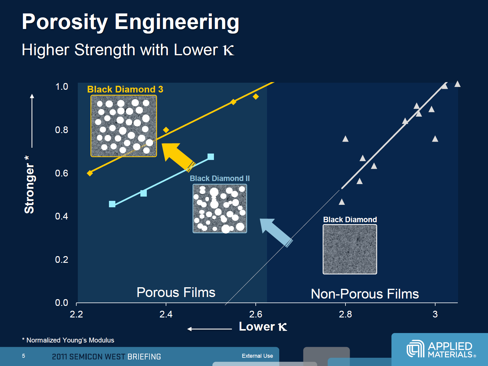
The last technical presentation (Bill McClintock) covered off the new Black Diamond 3 (BD3) and Nanocure 3 extreme low-k dielectric and curing combination, giving a dielectric constant (k) of 2.2, down from k=2.5 in the previous generation. One of the things he pointed out (that I hadn't thought about) was that the pre-metal dielectric layer at the bottom of the metal stack has to survive more than 150 process steps before wafer out in today's 10-12 metal-layer processes, never mind the stresses of the packaging and assembly sequence.


So the challenges are formidable as the k-value is pushed down, to get both physical and material integrity; AMAT claims that by going to a closed-pore structure, with tighter pore size distribution, they can achieve k=2.2.

According to Bill, we can expect to see BD3 at the 22/15 nm nodes, so a couple of years yet before we see it in high-volume products.

Then we got to the Q-and-A session. Ironically, the first question was not about any of the product launches -- it was about the spend on 450mm next year! Mike Splinter was reluctant to give a specific number, but he did say it would be "well over $100 million," mostly on early test systems in-house. Not exactly small change, all the same. A later question prompted the statements that "450 is going to happen," and that they are closely linked to the leading customers that will drive the move there. They are clearly now viewing 450mm as a strategic way of gaining market share when it does come.

Other questions covered off potential product expansion, and of course the future demand from foundries in what seems to be a softening market.

Randhir Thakur identified AMAT's flowable CVD, Siconi clean and the Raider copper deposition tools as having found more applications than originally intended. The flowable CVD was targeted on one application, but ended up replacing CVD fill for STI, and other CVD steps with high conformality requirements. Siconi clean has evolved from a PVD clean, but has now moved into CVD and epi areas, any area where interfaces are critical. The Raider copper tool was developed from a Semitool product for packaging, but now has potential for damascene copper on die.

When it comes to the foundries, it appears that the fab shells are ready, and the message for the equipment companies is to be ready -- things may be soft at the moment, but they could come back very quickly. Demand is controlled by the consumer market, and that has proved remarkably resilient considering some of the economic challenges in the last year or so.

All in all, an interesting session, both in the industry and technical senses. AMAT has the webcasts and presentations up on their investor website for until August 12, 2011.

Tuesday, July 12, 2011

TSMC HKMG is Out There!

I have to apologise for a hiatus in posting due to pressure from the day job, but this week is Semicon West week, so it seems appropriate to announce that we've started analysing TSMC's 28-nm gate-last HKMG product, in this case a Xilinx Kintex-7 FPGA, fabbed in TSMC's HPL process.

Having seen two generations of Intel's HKMG parts (the 45-nm Xeon and 32-nm Westmere) using gate-last technology, it's inevitable that we'll compare those with the TSMC process.

The Kintex family is the mid-range group in the latest 28-nm generation 7-series of FPGAs from the company. These are optimised for the highest price/performance benefit, giving the performance of the previous Virtex-6 parts at half the price.

The Kintex-7 has eleven layers of metal (Fig. 1); the 1x layers run from metals 1-4, with a pitch of ~96 nm, the smallest we have ever seen.

Fig. 1 General Structure of Xilinx Kintex-7

Contacted gate pitch is ~118 nm in our initial analysis, with minimum gate length of ~33 nm, though since this is replacement gate there is no way of knowing absolutely the original poly gate width, which defines the source/drain engineering.

Plan-view imaging (Fig. 2) indicates that TSMC has implemented the restricted design rules that have been much discussed in the gate-first/gate-last debate. Regular, uni-directional patterning of functional gate and dummy gate lines helps out the lithography, but inevitably reduces packing density compared with Manhattan layout schemes.

Fig.2 Plan-View Image of Gates and Active Silicon

By the look of it, double patterning with a gate plus a cut mask has been used. FPGAs are usually laid out in a more relaxed manner than dense logic, so here we can see lots of dummy gates, and also dummy active regions.

The gate structure itself definitely has some similarities with Intel's 45-nm, as we can see from figures 3 and 4.

Fig.3 Intel 45-nm (left) and TSMC/Xilinx 28-nm NMOS Transistors

Fig.4  Intel 45-nm (left) and TSMC/Xilinx 28-nm PMOS Transistors

In both it appears that the buffer oxide, the high-k layer and a common work-function material are put down before the sacrificial polysilicon gate. Then the source/drain engineering is performed, and dielectric stack deposited and planarized back to the polysilicon; and the sacrificial gate is removed, and the NMOS/PMOS gate stacks are put in and planarized.

Of course there are also differences – TSMC is not using embedded SiGe for PMOS strain, and there is an additional high-density metal layer in the PMOS gate. There is also no distinct dielectric capping layer in the TSMC structure, and there is an extra sidewall spacer (likely part of the source/drain tuning). The wafers are also rotated to give a <100> channel direction.

Intel stated that they applied stress to NMOS devices using the gate metal stack and the contacts; TSMC could be doing the same, although the contacts are spaced further from the gate edge. If there is PMOS stress, the mechanism is unclear, though it is possible that the extra high-density layer in the gate could be for that purpose. However, this part is fabbed in the HPL low-power process, and typically we do not see e-SiGe in such processes.

Analysis is ongoing – more details to come, and possibly a comparison with the AMD Llano gate-first HKMG part, that's in our labs at the moment.

N.B. We are at Semicon West, at Booth 2337 - drop by and get a coupon for a free die photo!


Wednesday, May 4, 2011

Intel Goes Tri-Gate at 22-nm!

In a pair of press and analyst briefings this morning, Mark Bohr and Steve Smith announced that Intel will indeed be using a 3D transistor structure for their 22-nm product, settling one of the big questions about Intel's process development over the last few years - do they stay planar or not? (And, incidentally, settling a bet between me and Scott Thompson - Scott wins!)

The big debate at IEDM last year about advanced CMOS was whether transistor structures would move to a 3D structure (finFET, tri-gate, whatever label you choose), or use ultra-thin SOI layers to attain fully depleted operation. The debate was not resolved - I was definitely left with the impression that the adherents in both camps held to their opinions, which probably means we will have two process groupings, much as we have with the gate-first/gate-last high-k/metal gate (HKMG) structures.

Intel have come down on the side of tri-gate - apparently the decision was taken in 2008, after their researchers had showed that the gate-last HKMG gate structure would work in 3D, and that the planar version could not give enough of a performance boost. So for the last three years they've been developing the process and getting it manufacturable for the production of the Ivybridge product line later this year.


Intel's Research and Development Sequence to Reach the Tri-Gate 22-nm Node

I may have lost the bet about planar, but my gut feel that their HKMG process could be extended to 22-nm seemed to be right, since Mark confirmed that they are using gate-last (replacement gate) technology, with evolutions of existing NMOS and PMOS strain technology. Immersion lithography and double patterning will be used where necessary, and no extra mask layers are needed so the additional cost is only 2 - 3%. And apparently it's scalable to 14 nm!

The schematic below shows a gate formed on three sides of three fins, to give more drive strength than available from one fin:

Schematic of Tri-Gate Across Three Fins (Source - Intel)

When translated to gate-last HKMG, it looks like this in this Intel image from 2007 (the section is through three gates, with three fins buried under oxide running across the field of view):

Gate-Last HKMG Tri-Gate Transistors (Source - Intel)

And now a new image from today's briefing, showing an array of transistors with six fins in the centre, and some with two fins at the top right and bottom left:

Intel Tri-Gate Transistors (with STI and gate mold oxide removed) (Source - Intel)

Clearly this means a whole new set of design and layout paradigms, and we can see evidence here of double patterning using fin and gate masks, with cut masks to define the individual fins and gates.

During the briefings, Mark also scotched the rumour that appeared a few weeks ago about a hybrid process, where the SRAM is tri-gate and other areas are planar - all of the chip area will be tri-gate. In addition a parallel SoC process is being developed so that the Atom line of products can be extended to 22-nm.

For us commentators, going tri-gate was always a possibility for Intel; they have been publishing papers on the topic for almost ten years, with a flurry of them five years ago - here's an image from a press briefing in 2006:

TEM Image of HKMG Tri-Gate Transistor, Sectioned Through the Fin(Source - Intel)

Their R-D-M (Research-Development-Manufacturing) methodology has been well established for quite a while now, and enabled them to keep to their schedule of a new process generation every two years. Based on comments today, we can expect to see 22-nm production in the second half of this year, and product on the shelves in the New Year.

Then we'll see what it really looks like!

Tuesday, April 26, 2011

A Shameless Plug for ASMC

Winter is finally starting to fade in Ottawa, and the early signs of spring are showing. The maple sap is running, the first migrant birds have arrived, the frogs are peeping, and we have evening daylight. On the conference calendar, spring means that ASMC (IEEE/SEMI Advanced Semiconductor Manufacturing Conference) is on the horizon, this year in Saratoga Springs, New York on May 16 -18. There, spring should be well advanced, and it will be a great time of year to visit the Empire State.

As the name says, ASMC is an annual conference focused on the manufacturing of semiconductor devices - in this it differs from other conferences, since the emphasis is on what goes on in the wafer fab, not the R&D labs, and the papers are not exclusively research papers.

I’m plugging ASMC because it seems to be one of the more under-rated conferences, unlike IEDM and the VLSI symposia, which get the media attention for leading-edge R&D and processes. However, it’s the nitty-gritty of manufacturing in the fab that gets the chips out of the door, and this meeting discusses the work that pushes the yield and volumes up and keeps them there.

I always come away impressed by the quality of the engineering involved; not being a fab person myself any more, it’s easy to get disconnected from the density of effort required to equip a fab, keep it running and bring new products/processes into production. Usually the guys in the fab only get publicity if something goes wrong!

This year, in addition to the 50-plus papers, there are keynotes from Norm Armour of GLOBALFOUNDRIES (GloFo), Gary Patton of IBM, and Peter Wright of Tradition Equities, as well as a panel discussion on partnerships in semiconductor manufacturing, moderated by Dave Lammers. There are also tutorials, on 3D (by James Lu of Rensselaer Poly), and EUV (by Obert Wood of GloFo), and an invited session of ISMI papers.

The technical sessions include:

  • Factory Optimization
  • Advanced Metrology
  • Advanced Equipment, Materials and Processes
  • Advanced Process Development and Control
  • Advanced Lithography
  • Defect Inspection and Yield Optimization
  • Data Management

Of course, I’m biased to some extent because we’ll be giving a paper there again. I can't make it this year, but a colleague of mine, Ray Fontaine, is presenting on "Recent Innovations in CMOS Image Sensors". This will be the seventh year running we’ve given a paper, the manufacturing and equipment engineers that attend seem to like seeing what their competitors are doing. In this case Ray will run through some of the changes in the camera chips that we all take for granted in our phones these days.

Other papers that caught my eye may give us some clues as to what to expect in the lithographic field; the IBM/Glofo/Toshiba alliance has one on contact patterning strategies (paper 6.3), and another cooperative paper by IBM/JSR/KLA Tencor/Tokyo Electron on double patterning (6.1), and an IBM/ASML contribution on advanced overlay control (2.5). And on the materials processing side, there are three papers on low-k dielectrics from GloFo/KLA Tencor (2.4), UAlbany/Air Liquide (3.5), and Novellus (poster in session 4); and a couple on nickel silicide by GloFo (5.3) and Ultratech (poster in session 4); and a clue to the mysteries of high-k dielectrics from UMC/National Cheng Kung U (3.4).

More stategically aimed discussions are by Infineon (1.1) on the challenges in having a global supply chain, Sumita Bas of Intel will be speaking on sustainable/green in the chip business (1.3), and two talks by SEMATECH, one on 450 mm manufacturing (ISMI session), and the other on 3D/TSV manufacturing (3.1).

Out of the conference room, there's a poster session and reception on the Monday evening, and on the Tuesday, Dave Lammers' panel session, "Models for Successful Partnerships in Semiconductor Manufacturing". Partnership is one of the buzzwords in chipmaking these days, and the panelists we have should know it well; Ari Komeran from the industry development side of Intel, Michael Fancher from Albany, Olivier Demolliens, head of LETI-NANOTEC in France; and Dr Walid Ali, from ATIC in Abu Dhabi.

After the panel session, what could be a highlight of the conference, a tour of the Luther Forest Technology Campus, including a look at GLOBALFOUNDRIES (Norm Armour's) new Fab 8, followed by a reception at the Canfield Casino.

Register soon - rates go up on May 8th!

Monday, March 21, 2011

Panasonic Gate-First HKMG also First Out of the Gate

As I suggested a few months ago, we put some credence in Panasonic’s press release last September that they would be shipping their first 32-nm HKMG parts last October. Samsung had announced their Saratoga chip, and both Altera and Xilinx have displayed silicon from TSMC, but until last Friday (18 March), none have said that they were shipping product. As of Friday Xilinx announced that they were shipping their Kintex-7 product, the first of their 7-series of FPGAs.

Earlier this month our faith in Panasonic was rewarded, and we found the chip! It took a few false starts buying Panasonic products that we tore down and threw away, but now we have a verified 32-nm, gate-first, high-k metal-gate (HKMG) product. The supply chain was a bit longer than we had hoped, but as promised the chip was shipped with a week 41 date code, in October.

So, for the curious, this is what a transistor looks like:

Panasonic's 32-nm HKMG NMOS Transistor

We can see the TiN metal gate at the base of the polysilicon, and the thin line of high-k at the base of the TiN. Also noticeable are a dual-spacer technology (sometimes referred to as differential offset spacers), and a thin line of nitride over the source/drain extension regions (possibly indicating a nitrided oxide under the high-k). The salicide is the usual platinum-doped nickel silicide. Less visible are mechanisms of applying strain, other than the nitride layer over the gate; embedded SiGe and dual-stress liners are not used.

All of which is typical for Panasonic – their 45-nm product did not appear to use any enhanced strain techniques, and the only concession to PMOS enhancement was wafer rotation to give a 1-0-0 channel direction. The emphasis is different from Intel; rather than raw performance, the targets are increased integration, die size reduction/reduced cost, and now we have high-k, reduced leakage/lower power. The September press release does say that transistor performance is improved by 40%, but it also claims 40% power reduction and a 30% smaller footprint.

Here’s a 45-nm transistor for comparison:

Panasonic's 45-nm Generation Transistor

And, for good measure, Intel's 32-nm device:

Intel 32-nm NMOS Transistor

The part itself uses a nine-metal (eight Cu, one Al) stack with a hybrid low-k/extra-low-k stack. Die size is ~45 mm2 in a conventional FC-BGA package. Minimum metal pitch is specified as 120 nm [1], and we have found 125 nm in our early investigations.

Panasonic 32 nm General Structure

Analysis is ongoing – stay tuned for more details, and of course we’ll be doing reports!

[1]S. Matsumoto et al., Highly Manufacturable ELK Integration Technology with Metal Hard Mask Process for High Performance 32nm-node Interconnect and Beyond”, IITC 2010

Sunday, March 13, 2011

Apple's A5 Processor is by Samsung, not TSMC

Forty-eight hours ago we obtained an iPad 2 and brought it back to the lab, and took it apart to have a look at Apple's A5 processor chip. We've come to the conclusion that the main innovation in the new iPad is the A5 chip. Flash memory is flash memory (multi-sourced from Samsung and Toshiba in the iPads we've seen), the DRAM in the A5 package is 512 MB instead of 256 MB, and the touchscreen control uses the same trio of chips as the iPad 1 – not even a single chip solution as we’ve seen in the later iPhones. And the 3G version uses the same chipset as the Verizon iPhone launched a few weeks ago. This is the mother-board from a 32-GB WiFi-only iPad 2:

Motherboard from 32-GB iPad 2


The A5 can be seen in the centre of the board. If we look at the package we can identify the Apple's APL0498 marking for the A5 (the A4 is APL0398), and also 4 Gb of Elpida mobile DRAM. Date codes are 1107 for the A5 and 1103 for the memory - only a few weeks in the supply chain here!


Apple A5 from iPad 2


The x-ray images show us that we have the usual package-on-package (PoP) structure, with two memory chips in the top part of the PoP, and the APL0498 processor on the lower half.


X-Ray Image of A5 Package-on-Package

The two rows of dense black dots on the outside of the image are the solder balls from the memory chips in the top half of the package (connecting with the bottom half), and the less dense dots are the solder balls on the bottom half of the package connecting the A5 chip to the iPad board below. If you squint really hard you can see smaller dots about five rows in from the edge which are the flip-chip solder balls on the A5 die – and they take up quite a large proportion of the area, showing that this is a good-sized die.
The die photo and die mark are shown here:
Die Photo of Apple's A5 Chip from the iPad 2

APL0498E01 Die Mark of Apple A5 Chip


The x-ray is right – the A5 die is more than twice as large as the A4, at 10.1 x 12.1 mm (122.2 mm2), vs 7.3 x 7.3 mm (53.3 mm2) – here’s the A4 chip for comparison:
Apple A4 Die Photo


Given that the A5 is a dual-ARM core, and has more graphics capability than the A4, more than doubling the size is to be expected, but it’s also a clue that this is still made in 45-nm technology.
So after the web speculation that TSMC might be fabbing the A5 rather than Samsung, we had to take a look, and the quickest way is to do a cross-section and compare it with the A4 from last year’s iPad.
So here’s the A5:
SEM Cross-Section of Apple A5
It’s a nine-metal layer part, with eight levels of copper and one aluminum. Zooming into the transistor level:
SEM Cross-Section of Transistors and M1 in A5 Processor
And now the A4:

SEM Cross-Section of Transistors and M1 - M4 in A4 Processor

At this scale even electron microscopes start to run out of steam, so not the clearest of images in either case, but good enough to see the similar shape of the transistor gates and the dielectric layers. So at least this sample of the A5 is fabbed by Samsung, just as all Apple’s processor chips have been for the last while.

Many thanks to the guys in the lab who've worked through the weekend to get this information - Chipworks is not really in the media business, but there's always a buzz when a hot new consumer part comes out.

And on a different note, commiserations and condolences to our Japanese colleagues, they have much more important things of concern than the details of the iPad 2.