On
the Monday afternoon at IEDM
the key paper for me was the Intel/Micron talk on their 3D-NAND flash part
(paper 3.3), which is currently sampling to customers. Samsung put their V-NAND
flash on the market last year, but that uses charge-trap technology, whereas
the Intel/Micron device has adapted conventional floating gate technology to
the vertical direction.
This is the first-generation product, with 32
active tiers plus additional layers for dummy wordlines and source and drain
select gates. A vertical channel surround-gate structure is used for the flash
cells. The CMOS decoders and sense-amps are situated under the NAND flash array,
which saves significantly on die area. It appears that this product will be a
256-Gb memory, or 384 Gb when the TLC version is introduced. Die size is 168.5
mm2, giving a bit density of 1.52 and 2.28 Gb/mm2 for the
MLC and TLC devices.
Intel/Micron 3D-NAND flash die (Source:
Intel/Micron/IEDM)


SEM cross-section of vertical-channel 3D-NAND
structure (Source: Intel/Micron/IEDM)
The process is shown below; the cell hole is first etched through the wordline tiers, and then the control gate is recessed back and the inter-poly dielectric is formed. The floating gate is then deposited, and etched back to form an isolated floating gate in each cell; the tunnel-oxide is formed, and the polySi channel is deposited to line the hole in the stack.

Process flow of vertical-channel 3D-NAND stack
formation (Source: Intel/Micron/IEDM)
An image of the full
stack is shown below; I see 38 wordline layers, plus a thick polySi layer at
top and bottom of the stack, presumably for the drain and source select
transistors. There are two tungsten metal layers below the stack for the decoders
and sense-amps, and also the wordline drivers; and it looks like the M3 bitline
is also tungsten. There is another metal level above used for power busses and
global interconnects, but we don’t know if that is copper or aluminum.
Putting the wordline
drivers under the array is claimed to keep the wordlines short, but it raises
some questions – how are the wordlines contacted from below? Do we have the
sort of staircase at the ends of the wordlines that we
saw in the Samsung V-NAND, and could it be inverted? (Can’t
imagine that!)

SEM cross-section of 3D-NAND stack (Source: Intel/Micron/IEDM)
|
M3 bitline
|
|
M2
|
|
NAND cell
stack
|
The vertical channels contact what looks like a
polySi sourceline at the base of the stack; it’s a bit clearer in this
schematic:

Schematic of base of 3D-NAND stack (Source: Intel/Micron/IEDM)
While the NAND cells
are floating gate cells, we can see that the source and drain select devices
are single gate oxide transistors.
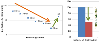
The larger size of the
cell improves the performance since it has a higher cell capacitance – more
electrons can be stored, and a better natural Vt distribution (~50%) is
achieved. (Note that at 20-nm planar, less than 10 electrons gave 100mv Vt
shift!)

Cell/cell interference of 3D-NAND vs planar NAND (Source: Intel/Micron/IEDM)
The cell geometry also means that the cell/cell interference is reduced – again, comparing to the 20-nm planar chip;

Cell/cell interference of 3D-NAND vs planar NAND (Source: Intel/Micron/IEDM)
We will see what the
commercial part looks like when we get our hands on one, likely in the first
few months of next year. Unfortunately there are no scale bars on any of the
images, so we have no feel for what the actual dimensions are; though probably
not too different from the Samsung, which is classed as a 40-nm device.
There are actually not
too many features in common with the Samsung chip – vertical stacking with 32
active layers, and that’s about it. Otherwise, charge-trap technology vs
floating-gate; polySi wordlines vs tungsten; metallization below the stack, vs
none; and maybe a completely different way of accessing the wordlines.
For now, we wait and
see!
No comments:
Post a Comment